SEMICONDUCTOR MATERIALS
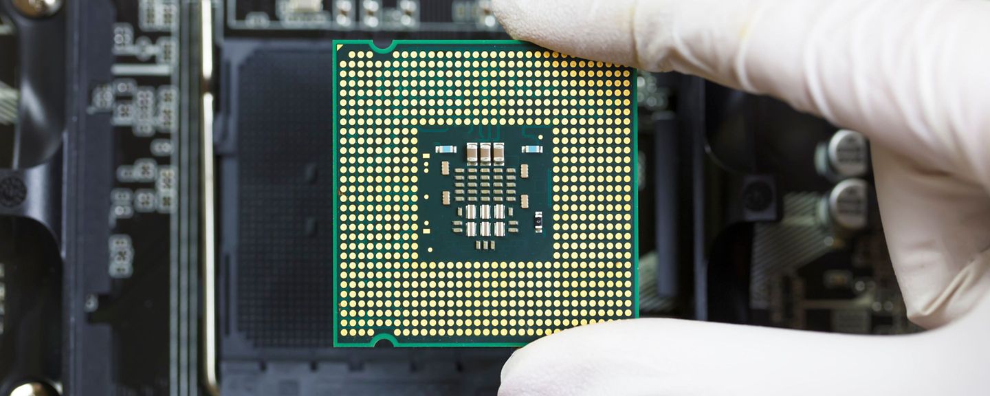
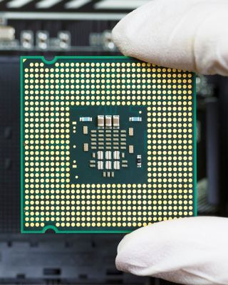
High-Performance Sputtering Targets
Engineered to enable the superior performance of your next-generation semiconductors
Stay Ahead with the Most Consistent, High-Quality Metals for Your Manufacturing Needs.
Keep your manufacturing running with the highest quality metals. As the world's largest manufacturer of sputtering targets for the semiconductor industry, we provide the most consistent microstructure control down to the sub-micron level, ensuring the lowest particulate counts in the industry. With increased production capacity and expertise in copper, cobalt, titanium, and tungsten, we meet the needs of most OEM designs in PVD applications. We have four major electronic materials centers focused on research and development: Spokane, Washington; Sunnyvale, California; Chonburi, Thailand and Shanghai, China.

Industry-leading Target composition for consistent sputtering: The high value-added advanced materials with the patented technologies meet the most demanding requirements in the semiconductor industry

Designed for usage in diverse applications: Intensive metallurgy experience and collaborations with partners, optimized for various end-user applications - be it real-time performance or sustained long-term reliability.

World-class manufacturing capabilities, supply chain, and sustainability support: Continuous investments in capacity expansion, process technology upgradation, and material recycling to meet the increasing industry demand.
Featured Products
With the core technologies to meet Target configurations and high-purity specifications, we have a strong position across metals.
Along with extensive Powder Processing experience, we have a strong position across other metals too:
- Tungsten
- Tungsten-alloy
- Titanium-alloy
- Tantalum-alloy
- Molybdenum
- Ruthenium
Ready To Connect?
Elevate your manufacturing process with our unparalleled metals, engineered for precision and reliability in the semiconductor industry. Our commitment to quality and innovation ensures that you have access to the materials that will keep your production lines running smoothly and efficiently. Don’t miss the opportunity to partner with us for your metal needs. Fill out the form below to get in touch with our experts and discover how we can support your manufacturing goals today!
